No products
Product successfully added to your shopping cart
There are 0 items in your cart. There is 1 item in your cart.
首頁
-
MCU
- 8bit 8051 MCUs
-
Arm Cortex-M0
- M0 Development Tool
- M091 Series
- M029G/M030G/M031G Series
- M031 Series
- M032 Series
- M071 Series
- M0A21 Series
- M0A23 Series
- NUC029 Series
- Nano103 Base Series
- Nano100/102 Base Series
- Nano110/112 LCD Series
- Nano120 USB Series (Ultra-Low Power)
- Nano130 LCD with USB Series (Ultra-Low Power)
- NUC100/200 Series
- NUC120/123 USB Series
- NUC121/125 Series
- NUC126 USB Series
- M051 Series
- Mini51 Series
- M0518 Series
- NUC131 CAN Series
- M0519 Series
- M0564 Series
- Arm Cortex-M23
-
Arm Cortex-M4
- M4 Development Tool
- M463 CAN FD/USB HS Series
- M467 Ethernet/Crypto Series
- M471 Series
- M487 Ethernet Series
- M485 Crypto Series
- M484 USB HS OTG Series
- M483 CAN Series
- M482 USB FS OTG Series
- M481 Base Series
- M4TK Series
- M451 Series
- NUC442/472 Series
- M452 USB Series
- M453 CAN Series (CAN+USB)
- NUC505 Series
- M433 CAN/USB FS OTG Series
- Arm Cortex-M33
- Arm Cortex-M55
- Arm Cortex-M7
- MPU
- Audio
- Application
- Tool
- Laser Diodes
- Analog ICs
- Motor
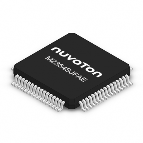
M2354SJFAE
| Quantity | Unit Price (USD) | |
| 1-99 | 5.03 | |
| 100-499 | 3.86 | |
| 500-999 | 3.22 | |
| 1000-1999 | 2.91 | |
| 2000-4999 | 2.81 | |
| 5000+ | Contact | |
The NuMicro® M2354 Series is a TrustZone® for Arm®v8-M architecture empowered microcontroller series focusing on IoT Security based on Arm® Cortex®-M23 CPU core technology. It runs up to 96 MHz with 1024 Kbytes embedded Flash memory and 256 Kbytes SRAM, supporting Flash in dual-bank mode, secure firmware OTA (Over-The-Air) update, ultra-low power consumption in normal run with 89.3 uA/MHz in LDO mode, 39.6 uA/MHz in DC-DC mode and and an 8x40/ COMxSEG LCD driver inside. Besides the fundamental microcontroller security features, it further enhances the chip-level security in covering side-channel attacks mitigation to crypto hardware engine, fault injection mitigation for operating voltage and clock as well as active shield to cryptographic key storage. The series supports power supply voltage from 1.7V ~ 3.6V in operating temperature range from -40°C to 105°C, and is equipped with both LDO and DC-DC power supply functionalities. The M2354 Series is quite competitive for those devices that need more secure, fast computing and low power in the IoT market.
Key Features:
| • | Security Core | ||
| - | Arm® Cortex®-M23 core Based | ||
| - | TrustZone® for ARM®v8-M | ||
| - | 32-bit Single-cycle hardware multiplier | ||
| - | 32-bit 17-cycle hardware divider | ||
| - | Up to 8 regions MPU_NS (for non-secure world) | ||
| - | Up to 8 regions MPU_S (for secure world) | ||
| - | 8 Security Attribution Unit (SAU) memory regions | ||
| • | Memories | ||
| - | 1 MB Dual-Bank Flash memory, allowing read-while-write | ||
| - | 256 KB SRAM,first 32 KB SRAM with hardware parity check | ||
| 16 KB Secure Boot ROM | |||
| - | 16 KB Flash User Loader (LDROM) | ||
| - | 8 KB Data Flash (with Data Scrambling) | ||
| - | 2 KB Flash for Secure Key storage | ||
| - | 3 KB OTP memory for General Purpose (3KB data + 1 KB lock bit) | ||
| - | 12 KB Secret OTP memory for Platform Security (root keys, product lifecycle management, firmware version control) | ||
| - | ISP / ICP / IAP programming | ||
| • | Power management | ||
| - | Normal run:89.3 μA/ MHz (LDO) ; 39.6 μA/ MHz (DC-DC) | ||
| - | Idle mode : 31.5 μA/ MHz (CPU clock disabled, LDO) ; 14.3 μA/ MHz (CPU clock disabled, DC-DC) | ||
| - | Power-down:20 μA | ||
| - | Standby power-down:2.0 μA | ||
| - | Deep power-down:0.5 μA (with VBAT) | ||
| - | Deep power-down:0.1 μA (VBAT) | ||
| - | VBAT supply for RTC:0.5 μA (80 bytes spare registers) | ||
| • | Crypto and Security | ||
| - | True random number generator (TRNG) | ||
| - | AES-256/ SHA-512/ HMAC-512 (AES with CCM, GCM, GMAC modes) | ||
| - | RSA-4096 | ||
| - | The ECC accelerator is a fully compliant implementation for the prime field GF (p) and binary field GF (2m) algorithms. The prime field GF (p) supports up to NIST P-521. The binary field GF (2m) supports up to NIST B-571 and NIST K-163, K-233, K-283, K - 409, and K-571. | ||
| - | SM2/ SM3/ SM4 (Chinese national cryptography standards) | ||
| - | CRC calculation unit | ||
| • | Communication interfaces | ||
| - | Up to 11 UART interfaces (up to10.66 MHz) ,with up to 3 ISO-7816-3 interfaces, 6 RS-485、2 USCI,and 2 LIN interfaces | ||
| - | Up to 5 I²C interfaces (up to 1 Mbps), with up to 3 I²C with SM Bus/ PM Bus、2 USCI | ||
| - | Up to 7 SPI interfaces (up to 64 MHz), with 4 I²S interfaces, additional 1 Quad-SPI interfaces, 2 USCI | ||
| - | Up to 4 I²S interfaces,3 I²S shared with 3 SPI | ||
| - | Secure Digital I/O (SDIO) (up to 50 MHz) | ||
| • | Advanced connectivity | ||
| - | USB 2.0 full speed OTG controller with on-chip PHY | ||
| - | One CAN interface up to 1 Mbps ( CAN 2.0A and 2.0B) | ||
| - | Crystal-less USB | ||
| - | 8 x 13 COM/SEG Segment LCD Display | ||
| • | Operating Characteristics | ||
| - | Running up to 96 MHz | ||
| - | Voltage range: 1.7V to 3.6 V | ||
| - | Temperature range: -40°C to 105°C | ||
| - | Selectable core power voltage levels: 1.26V or 1.2V in run and idle mode | ||
| • | Packages (RoHS) | ||
| - | LQFP 64-pin | ||
For more details and documents, please link to Nuvoton Official Website GO
-
| Quantity | Discount | You Save |
|---|---|---|
| 100 | 23.2% | Up to$116.70 |
| 500 | 36% | Up to$905.40 |
| 1000 | 42% | Up to$2,112.60 |
| 2000 | 44% | Up to$4,426.40 |
| Part No. | M2354SJFAE |
30 other products in the same category:
-
N572F072G
-
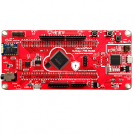
NuMaker-PFM-M2351
-
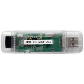
NU-ISDMINUSB
-
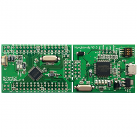
NuTiny-NUC029SDE
-
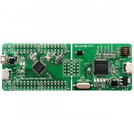
NuTiny-NUC029SEE
-
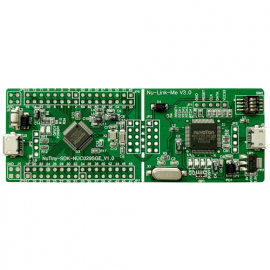
NuTiny-NUC029SGE
-
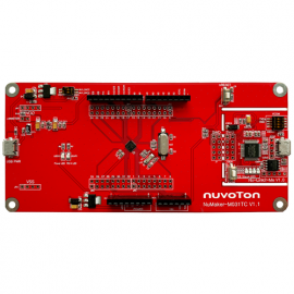
NuMaker-M031TC
-
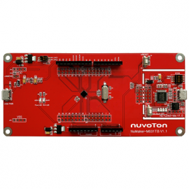
NuMaker-M031TB
-
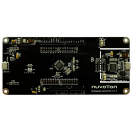
NuMaker-ML51PC
-
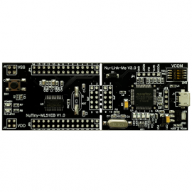
NuTiny-ML51EB
-
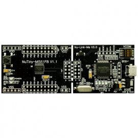
NuTiny-MS51FB
-
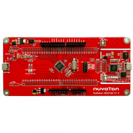
NuMaker-M031SD
-
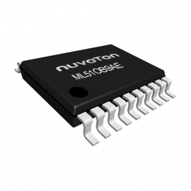
ML51OB9AE
-
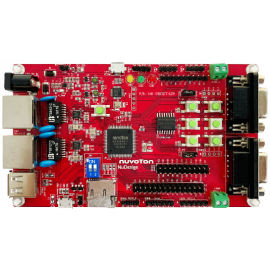
NuMaker-Server-NUC980
-

ML51UB9AE
-
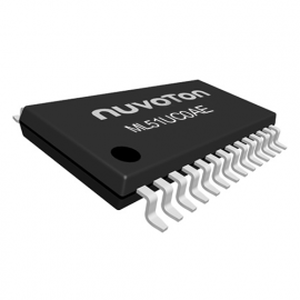
ML51UC0AE
-
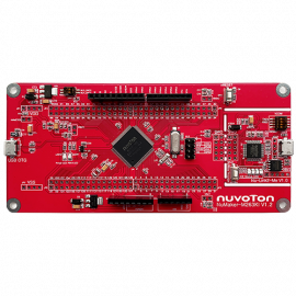
NuMaker-M263KI
-

M261ZIAAE
-
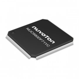
NUC980DF71YC
-

M261SIAAE
-

M261KIAAE
-
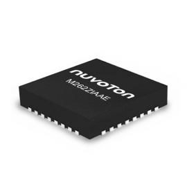
M262ZIAAE
-
M262SIAAE
-
M262KIAAE
-

M263ZIAAE
-

M263SIAAE
-

M263KIAAE
-
NuMaker-IIoT-NUC980
-
NuMaker-M483KG
-
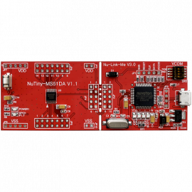
NuTiny-MS51DA

